Analysis of Electrical Networks with the Laplace Transform
Sources:
- B. P. Lathi & Roger Green. (2018). Chapter 4: The Laplace Transform. Signal Processing and Linear Systems (3rd ed., pp. 373-386). Oxford University Press.
We now show that it is also possible to analyze electrical networks directly without having to write the integro-differential equations. This procedure is considerably simpler because it permits us to treat an electrical network as if it were a resistive network. For this purpose, we need to represent a network in the "frequency domain" where all the voltages and currents are represented by their Laplace transforms.
For the sake of simplicity, let us first discuss the case with zero initial conditions.
For inductor
If \(v(t)\) and \(i(t)\) are the voltage across and the current through an inductor of \(L\) henries, then \[ v(t)=L \frac{d i(t)}{d t} \]
The Laplace transform of this equation (assuming zero initial current) is \[ V(s)=L s I(s) \]
For capacitor
Similarly, for a capacitor of \(C\) farads, the voltage-current relationship is \(i(t)=C(d v / d t)\) and its Laplace transform, assuming zero initial capacitor voltage, yields \(I(s)=C s V(s)\); that is, \[ V(s)=\frac{1}{C s} I(s) \]
For resistor
For a resistor of \(R\) ohms, the voltage-current relationship is \(v(t)=R i(t)\), and its Laplace transform is \[ V(s)=R I(s) \]
Summary
# TODO: What is impedance?
Thus, in the "frequency domain," the voltage-current relationships of an inductor and a capacitor are algebraic; these elements behave like resistors of "resistance" \(L s\) and \(1 / C s\), respectively. The generalized "resistance" of an element is called its impedance and is given by the ratio \(V(s) / I(s)\) for the element (under zero initial conditions).
The impedances of a resistor of \(R\) ohms, an inductor of \(L\) henries, and a capacitance of \(C\) farads are \(R, L s\), and \(1 / C s\), respectively.
Also, the interconnection constraints (Kirchhoff's laws) remain valid for voltages and currents in the frequency domain. To demonstrate this point, let \(v_j(t)(j=1,2, \ldots, k)\) be the voltages across \(k\) elements in a loop and let \(i_j(t)(j=1,2, \ldots, m)\) be the \(j\) currents entering a node. Then \[ \sum_{j=1}^k v_j(t)=0 \quad \text { and } \quad \sum_{j=1}^m i_j(t)=0 \]
Now if \[ v_j(t) \Longleftrightarrow V_j(s) \quad \text { and } \quad i_j(t) \Longleftrightarrow I_j(s) \] then \[ \sum_{j=1}^k V_j(s)=0 \quad \text { and } \quad \sum_{j=1}^m I_j(s)=0 \]
This result shows that if we represent all the voltages and currents in an electrical network by their Laplace transforms, we can treat the network as if it consisted of the "resistances" \(R, L s\), and \(1 / C s\) corresponding to a resistor \(R\), an inductor \(L\), and a capacitor \(C\), respectively. The system equations (loop or node) are now algebraic. Moreover, the simplification techniques that have been developed for resistive circuits-equivalent series and parallel impedances, voltage and current
Transform analysis of a simple circuit
Find the loop current \(i(t)\) in the circuit shown in Fig. 4.10a if all the initial conditions are zero.
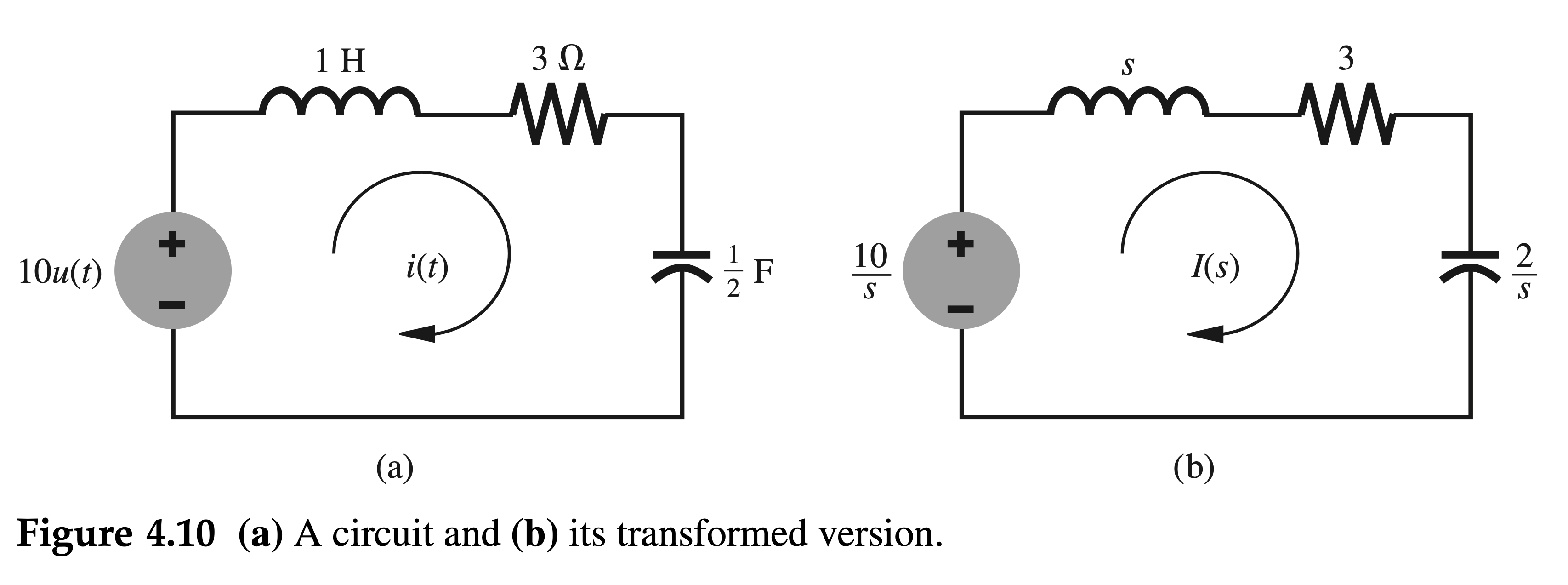
In the first step, we represent the circuit in the frequency domain, as illustrated in Fig. 4.10b.
All the voltages and currents are represented by their Laplace transforms. The voltage \(10 u(t)\) is represented by \(10 / s\) and the (unknown) current \(i(t)\) is represented by its Laplace transform \(I(s)\).
All the circuit elements are represented by their respective impedances. The inductor of 1 henry is represented by \(s\), the capacitor of \(1 / 2\) farad is represented by \(2 / s\), and the resistor of 3 ohms is represented by 3 . We now consider the frequency-domain representation of voltages and currents. The voltage across any element is \(I(s)\) times its impedance.
Therefore, the total voltage drop in the loop is \(I(s)\) times the total loop impedance, and it must be equal to \(V(s)\), (transform of) the input voltage. The total impedance in the loop is \[ Z(s)=s+3+\frac{2}{s}=\frac{s^2+3 s+2}{s} \]
The input"voltage" is \(V(s)=10 / s\). Therefore, the "loop current" \(I(s)\) is \[ I(s)=\frac{V(s)}{Z(s)}=\frac{10 / s}{\left(s^2+3 s+2\right) / s}=\frac{10}{s^2+3 s+2}=\frac{10}{(s+1)(s+2)}=\frac{10}{s+1}-\frac{10}{s+2} \]
The inverse transform of this equation yields the desired result: \[ i(t)=10\left(e^{-t}-e^{-2 t}\right) u(t) \]
Initial condition generators
The discussion in which we assumed zero initial conditions can be readily extended to the case of nonzero initial conditions because the initial condition in a capacitor or an inductor can be represented by an equivalent source.
We now show that a capacitor \(C\) with an initial voltage \(v\left(0^{-}\right)\) (Fig. 4.11a) can be represented in the frequency domain by:
- an uncharged capacitor of impedance \(1 / C s\) in series with a voltage source of value \(v\left(0^{-}\right) / s\) (Fig. 4.11b), or
- as the same uncharged capacitor in parallel with a current source of value \(C v\left(0^{-}\right)\)(Fig. 4.11c).
Similarly, an inductor \(L\) with an initial current \(i\left(0^{-}\right)\)(Fig. 4.11d) can be represented in the frequency domain by
- an inductor of impedance \(L s\) in series with a voltage source of value \(L i\left(0^{-}\right)\)(Fig. 4.11e), or by
- the same inductor in parallel with a current source of value \(i\left(0^{-}\right) / s\) (Fig. 4.11f).
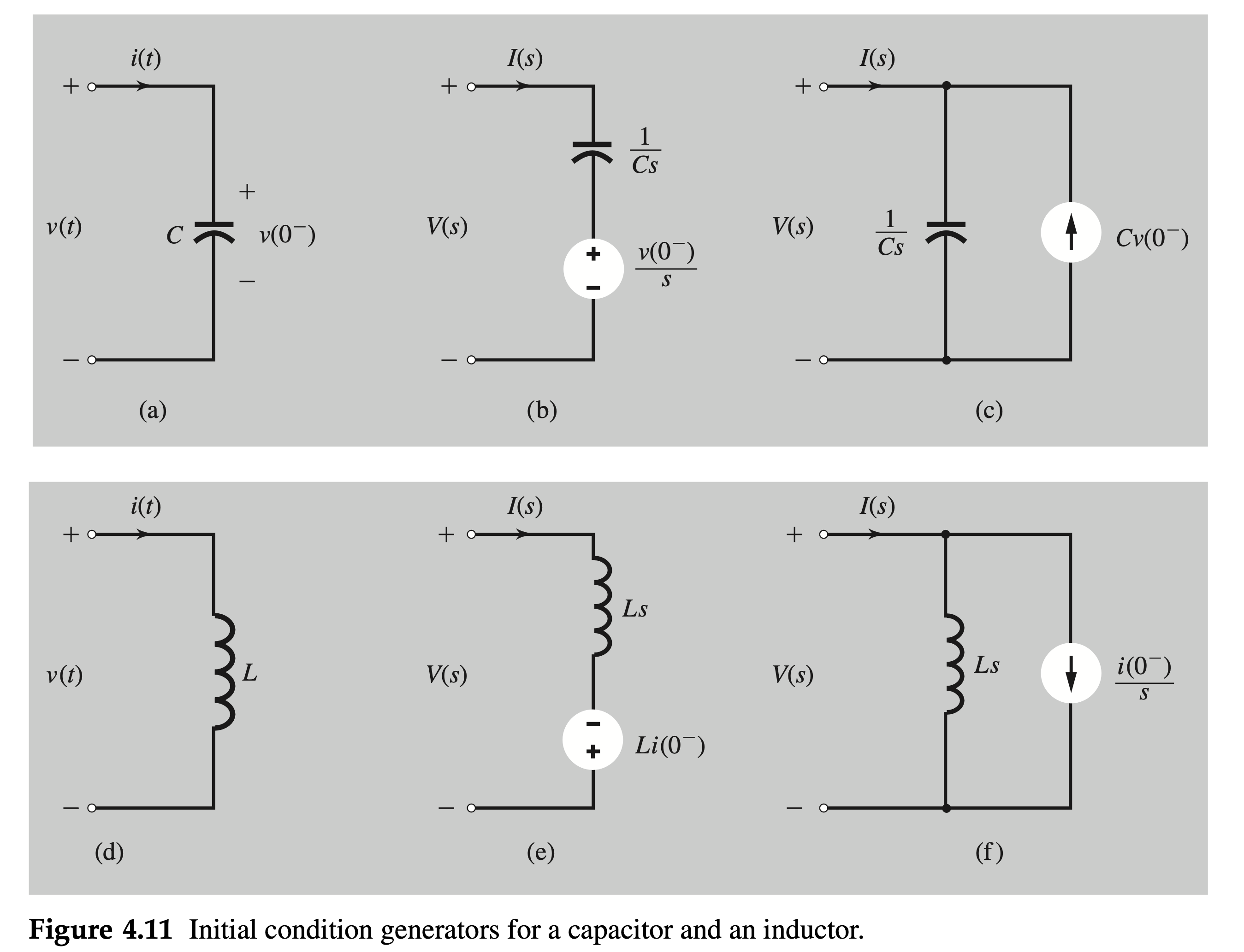
To prove this point, consider the terminal relationship of the capacitor in Fig. 4.11a: \[ i(t)=C \frac{d v(t)}{d t} \]
The Laplace transform of this equation yields \[ I(s)=C\left[s V(s)-v\left(0^{-}\right)\right] \] This equation can be rearranged as \[ \begin{equation} \label{eq4_33} \color{pink} {V(s)=\frac{1}{C s} I(s)+\frac{v\left(0^{-}\right)}{s}} \end{equation} \]
Observe that \(V(s)\) is the voltage (in the frequency domain) across the charged capacitor and \(I(s) / C s\) is the voltage across the same capacitor without any charge. Therefore, the charged capacitor can be represented by the uncharged capacitor in series with a voltage source of value \(v\left(0^{-}\right) / s\), as depicted in Fig. 4.11b.
\(\eqref{eq4_33}\) can also be rearranged as \[ \color{purple} {V(s)=\frac{1}{C s}\left[I(s)+C v\left(0^{-}\right)\right]} \]
This equation shows that the charged capacitor voltage \(V(s)\) is equal to the uncharged capacitor voltage caused by a current \(I(s)+C v\left(0^{-}\right)\). This result is reflected precisely in Fig. 4.11c, where the current through the uncharged capacitor is \(I(s)+C v\left(0^{-}\right)\).
For the inductor in Fig. 4.11d, the terminal equation is \[ v(t)=L \frac{d i(t)}{d t} \] and \[ \color{orange} {V(s)=L\left[s I(s)-i\left(0^{-}\right)\right]=\operatorname{LsI}(s)-\operatorname{Li}\left(0^{-}\right)} \]
This expression is consistent with Fig. 4.11e. We can it as \[ \color{brown} {V(s)=L s\left[I(s)-\frac{i\left(0^{-}\right)}{s}\right]} \]
This expression is consistent with Fig, 4.11f.
Transformed analysis of a circuit with a switch
The switch in the circuit of Fig. 4.13a is in the closed position for a long time before \(t=0\), when it is opened instantaneously. Find the currents \(y_1(t)\) and \(y_2(t)\) for \(t \geq 0\).
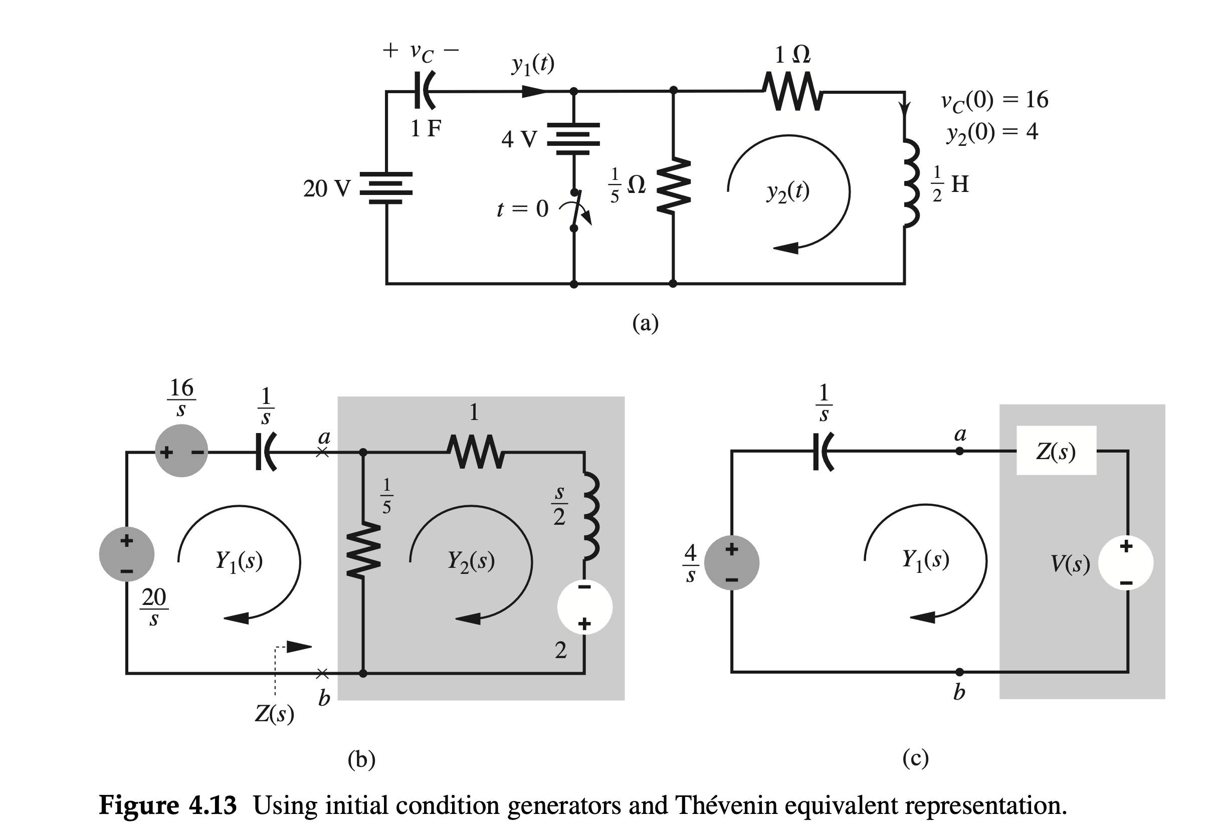
Inspection of this circuit shows that when the switch is closed and the steady-state conditions are reached, the capacitor voltage \(v_C=16\) volts, and the inductor current \(y_2=4\) amperes. Therefore, when the switch is opened (at \(t=0)\), the initial conditions are \(v_C\left(0^{-}\right)=16\) and \(y_2\left(0^{-}\right)=4\). Figure \(4.13 \mathrm{~b}\) shows the transformed version of the circuit in Fig. 4.13a. We have used equivalent sources to account for the initial conditions. The initial capacitor voltage of 16 volts is represented by a series voltage of \(16 / s\) and the initial inductor current of 4 amperes is represented by a source of value \(L y_2\left(0^{-}\right)=2\). From Fig. 4.13b, the loop equations can be written directly in the frequency domain as \[ \begin{aligned} \frac{Y_1(s)}{s}+\frac{1}{5}\left[Y_1(s)-Y_2(s)\right] & =\frac{4}{s} \\ -\frac{1}{5} Y_1(s)+\frac{6}{5} Y_2(s)+\frac{s}{2} Y_2(s) & =2 \\ {\left[\begin{array}{cc} \frac{1}{s}+\frac{1}{5} & -\frac{1}{5} \\ -\frac{1}{5} & \frac{6}{5}+\frac{s}{2} \end{array}\right]\left[\begin{array}{l} Y_1(s) \\ Y_2(s) \end{array}\right] } & =\left[\begin{array}{l} \frac{4}{s} \\ 2 \end{array}\right] \end{aligned} \]
Application of Cramer's rule to this equation yields \[ Y_1(s)=\frac{24(s+2)}{s^2+7 s+12}=\frac{24(s+2)}{(s+3)(s+4)}=\frac{-24}{s+3}+\frac{48}{s+4} \] and \[ y_1(t)=\left(-24 e^{-3 t}+48 e^{-4 t}\right) u(t) \]
Similarly, we obtain \[ Y_2(s)=\frac{4(s+7)}{s^2+7 s+12}=\frac{16}{s+3}-\frac{12}{s+4} \] and \[ y_2(t)=\left(16 e^{-3 t}-12 e^{-4 t}\right) u(t) \]
We also could have used Thévenin's theorem to compute \(Y_1(s)\) and \(Y_2(s)\) by replacing the circuit to the right of the capacitor (right of terminals \(a b\) ) with its Thévenin equivalent, as shown in Fig. 4.13c. Figure 4.13b shows that the Thévenin impedance \(Z(s)\) and the Thévenin source \(V(s)\) are \[ \begin{aligned} & Z(s)=\frac{\frac{1}{5}\left(\frac{s}{2}+1\right)}{\frac{1}{5}+\frac{s}{2}+1}=\frac{s+2}{5 s+12} \\ & V(s)=\frac{-\frac{1}{5}}{\frac{1}{5}+\frac{s}{2}+1} 2=\frac{-4}{5 s+12} \end{aligned} \]
According to Fig. 4.13c, the current \(Y_1(s)\) is given by \[ Y_1(s)=\frac{\frac{4}{s}-V(s)}{\frac{1}{s}+Z(s)}=\frac{24(s+2)}{s^2+7 s+12} \] which confirms the earlier result. We may determine \(Y_2(s)\) in a similar manner.
Transformed analysis of a coupled inductive network
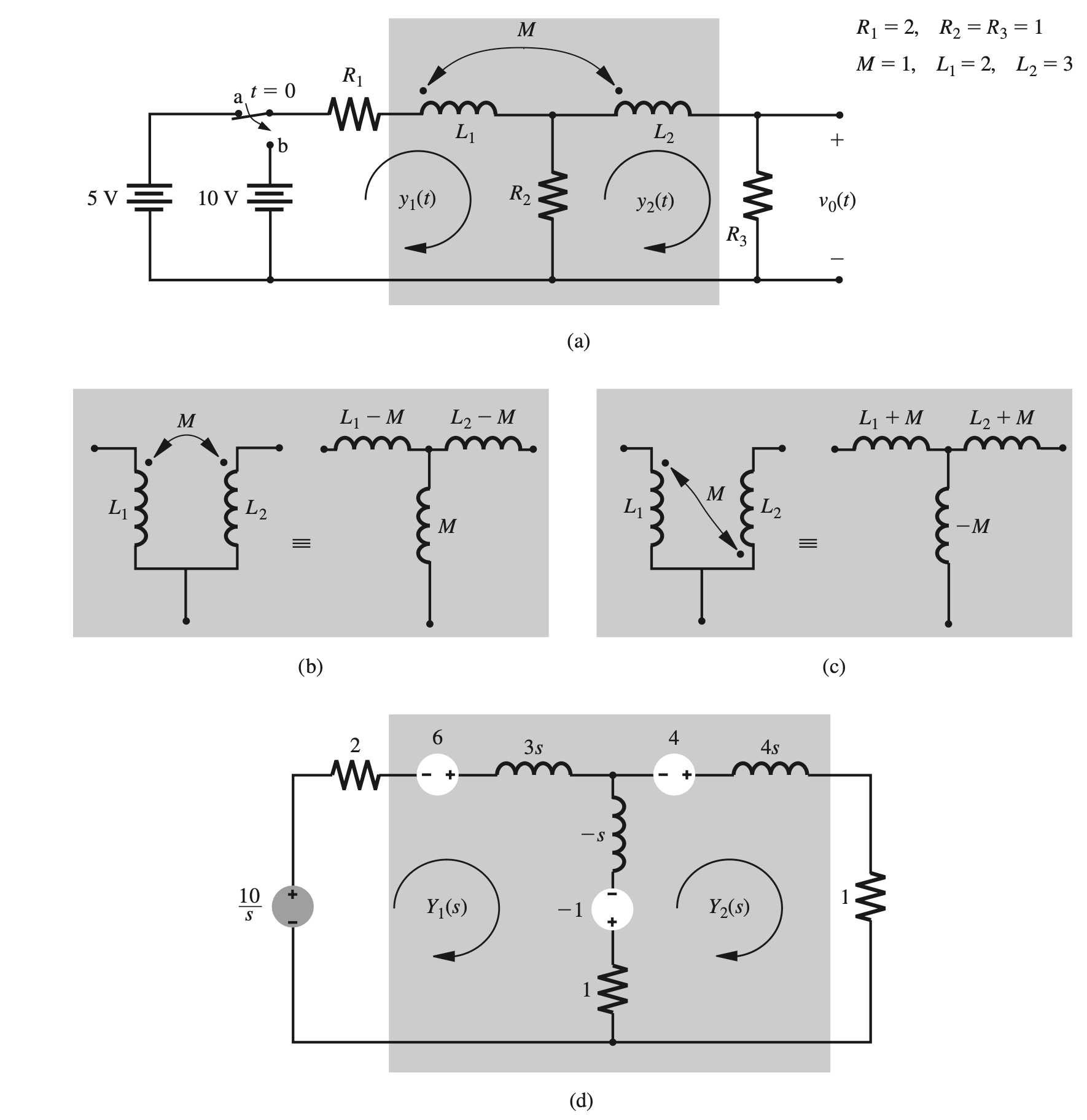
The switch in the circuit in Fig. 4.14a is at position a for a long time before \(t=0\), when it is moved instantaneously to position b. Determine the current \(y_1(t)\) and the output voltage \(v_0(t)\) for \(t \geq 0\). Just before switching, the values of the loop currents are 2 and 1 , respectively, that is, \(y_1\left(0^{-}\right)=2\) and \(y_2\left(0^{-}\right)=1\). The equivalent circuits for two types of inductive coupling are illustrated in Figs. 4.14b and 4.14c. For our situation, the circuit in Fig. 4.14c applies. Figure 4.14d shows the transformed version of the circuit in Fig. 4.14a after switching. Note that the inductors \(L_1+M, L_2+M\), and \(-M\) are 3,4 , and -1 henries with impedances \(3 s, 4 s\), and \(-s\) respectively. The initial condition voltages in the three branches are \(\left(L_1+M\right) y_1\left(0^{-}\right)=6,\left(L_2+M\right) y_2\left(0^{-}\right)=4\), and \(-M\left[y_1\left(0^{-}\right)-y_2\left(0^{-}\right)\right]=-1\), respectively. The two loop equations of the circuit are \[ \begin{aligned} & (2 s+3) Y_1(s)+(s-1) Y_2(s)=\frac{10}{s}+5 \\ & (s-1) Y_1(s)+(3 s+2) Y_2(s)=5 \end{aligned} \] or \[ \left[\begin{array}{cc} 2 s+3 & s-1 \\ s-1 & 3 s+2 \end{array}\right]\left[\begin{array}{l} Y_1(s) \\ Y_2(s) \end{array}\right]\left[\begin{array}{c} \frac{5 s+10}{s} \\ 5 \end{array}\right] \]
Solving for \(Y_1(s)\), we obtain \[ Y_1(s)=\frac{2 s^2+9 s+4}{s\left(s^2+3 s+1\right)}=\frac{4}{s}-\frac{1}{s+0.382}-\frac{1}{s+2.618} \]
Therefore, \[ y_1(t)=\left(4-e^{-0.382 t}-e^{-2.618 t}\right) u(t) \]
Similarly, \[ Y_2(s)=\frac{s^2+2 s+2}{s\left(s^2+3 s+1\right)}=\frac{2}{s}-\frac{1.618}{s+0.382}+\frac{0.618}{s+2.618} \] and \[ y_2(t)=\left(2-1.618 e^{-0.382 t}+0.618 e^{-2.618 t}\right) u(t) \]
The output voltage is therefore \[ v_0(t)=y_2(t)=\left(2-1.618 e^{-0.382 t}+0.618 e^{-2.618 t}\right) u(t) \]
Analysis of active circuits
Although we have considered examples of only passive networks so far, the circuit analysis procedure using the Laplace transform is also applicable to active circuits. All that is needed is to replace the active elements with their mathematical models (or equivalent circuits) and proceed as before.
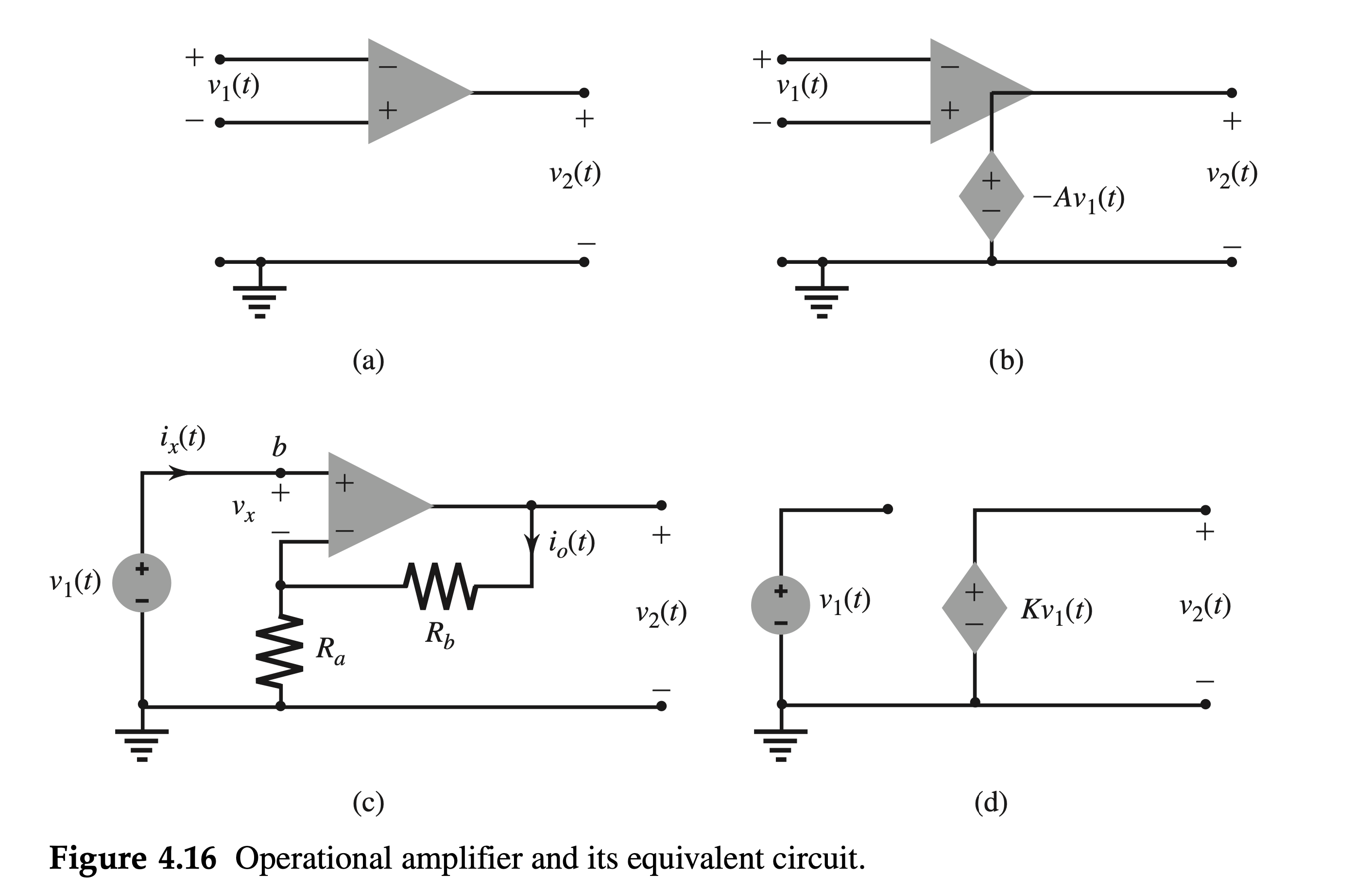
The operational amplifier (depicted by the triangular symbol in Fig. 4.16a) is a well-known element in modern electronic circuits. The terminals with the positive and the negative signs correspond to noninverting and inverting terminals, respectively. This means that the polarity of the output voltage \(v_2\) is the same as that of the input voltage at the terminal marked by the positive sign (noninverting). The opposite is true for the inverting terminal, marked by the negative sign.
Figure 4.16b shows the model (equivalent circuit) of the operational amplifier (op amp) in Fig. 4.16a. A typical op amp has a very large gain. The output voltage \(v_2=-A v_1\), where \(A\) is typically \(10^5\) to \(10^6\). The input impedance is very high, of the order of \(10^{12} \Omega\), and the output impedance is very low \((50-100 \Omega\) ). For most applications, we are justified in assuming the gain \(A\) and the input impedance to be infinite and the output impedance to be zero. For this reason we see an ideal voltage source at the output.
Consider now the operational amplifier with resistors \(R_a\) and \(R_b\) connected, as shown in Fig. 4.16c. This configuration is known as the noninverting amplifier. Observe that the input polarities in this configuration are inverted in comparison to those in Fig. 4.16a. We now show that the output voltage \(v_2\) and the input voltage \(v_1\) in this case are related by \[ v_2=K v_1, \quad \text { where } K=1+\frac{R_b}{R_a} \]
First, we recognize that because the input impedance and the gain of the operational amplifier approach infinity, the input current \(i_x\) and the input voltage \(v_x\) in Fig. 4.16c are infinitesimal and may be taken as zero. The dependent source in this case is \(A v_x\) instead of \(-A v_x\) because of the input polarity inversion. The dependent source \(A v_x\) (see Fig. 4.16b) at the output will generate current \(i_o\), as illustrated in Fig. 4.16c. Now \[ v_2=\left(R_b+R_a\right) i_o \]
and also \[ v_1=v_x+R_a i_o=R_a i_o \]
Therefore, \[ \frac{v_2}{v_1}=\frac{R_b+R_a}{R_a}=1+\frac{R_b}{R_a}=K \] or \[ v_2(t)=K v_1(t) \]
The equivalent circuit of the noninverting amplifier is depicted in Fig. 4.16d.
Transform Analysis of a Sallen-Key Circuit
The circuit in Fig. 4.17a is called the Sallen-Key circuit, which is frequently used in filter design. Find the transfer function \(H(s)\) relating the output voltage \(v_o(t)\) to the input voltage \(v_i(t)\).
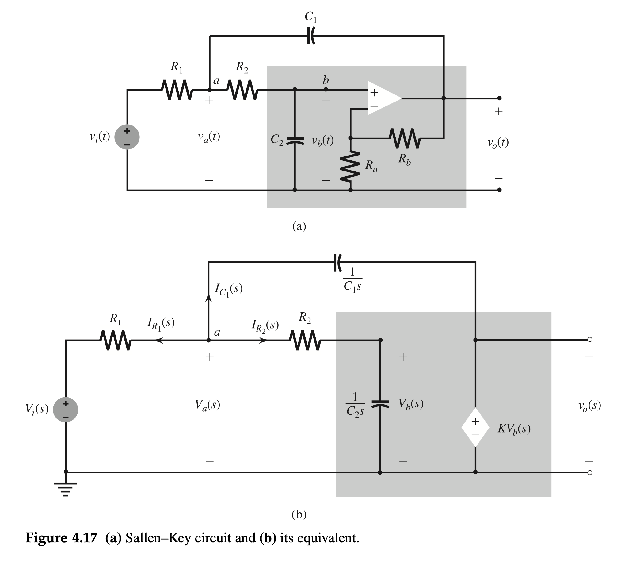
We are required to find \[ H(s)=\frac{V_o(s)}{V_i(s)} \] assuming all initial conditions to be zero. Figure 4.17b shows the transformed version of the circuit in Fig. 4.17a. The noninverting amplifier is replaced by its equivalent circuit. All the voltages are replaced by their Laplace transforms, and all the circuit elements are shown by their impedances. All the initial conditions are assumed to be zero, as required for determining \(H(s)\).
We shall use node analysis to derive the result. There are two unknown node voltages, \(V_a(s)\) and \(V_b(s)\), requiring two node equations.
At node \(a, I_{R_1}(s)\), the current in \(R_1\) (leaving the node \(a\) ), is \(\left[V_a(s)-V_i(s)\right] / R_1\). Similarly, \(I_{R_2}(s)\), the current in \(R_2\) (leaving the node \(a\) ), is \(\left[V_a(s)-V_b(s)\right] / R_2\), and \(I_{C_1}(s)\), the current in capacitor \(C_1\) (leaving the node \(a\) ), is \(\left[V_a(s)-V_o(s)\right] C_1 s=\left[V_a(s)-K V_b(s)\right] C_1 s\).
The sum of all the three currents is zero. Therefore, \[ \frac{V_a(s)-V_i(s)}{R_1}+\frac{V_a(s)-V_b(s)}{R_2}+\left[V_a(s)-K V_b(s)\right] C_1 s=0 \] or \[ \left(\frac{1}{R_1}+\frac{1}{R_2}+C_1 s\right) V_a(s)-\left(\frac{1}{R_2}+K C_1 s\right) V_b(s)=\frac{1}{R_1} V_i(s) \]
Similarly, the node equation at node \(b\) yields \[ \frac{V_b(s)-V_a(s)}{R_2}+C_2 s V_b(s)=0 \] or \[ -\frac{1}{R_2} V_a(s)+\left(\frac{1}{R_2}+C_2 s\right) V_b(s)=0 \]
The two node equations in two unknown node voltages \(V_a(s)\) and \(V_b(s)\) can be expressed ir matrix form as \[ \left[\begin{array}{cc} G_1+G_2+C_1 s & -\left(G_2+K C_1 s\right) \\ -G_2 & \left(G_2+C_2 s\right) \end{array}\right]\left[\begin{array}{l} V_a(s) \\ V_b(s) \end{array}\right]=\left[\begin{array}{c} G_1 V_i(s) \\ 0 \end{array}\right] \] where \[ G_1=\frac{1}{R_1} \quad \text { and } \quad G_2=\frac{1}{R_2} \]
Application of Cramer's rule yields \[ \begin{aligned} \frac{V_b(s)}{V_i(s)} & =\frac{G_1 G_2}{C_1 C_2 s^2+\left[G_1 C_2+G_2 C_2+G_2 C_1(1-K)\right] s+G_1 G_2} \\ & =\frac{\omega_0^2}{s^2+2 \alpha s+\omega_0^2} \end{aligned} \] where \[ \begin{gathered} K=1+\frac{R_b}{R_a} \quad \text { and } \quad \omega_0{ }^2=\frac{G_1 G_2}{C_1 C_2}=\frac{1}{R_1 R_2 C_1 C_2} \\ 2 \alpha=\frac{G_1 C_2+G_2 C_2+G_2 C_1(1-K)}{C_1 C_2}=\frac{1}{R_1 C_1}+\frac{1}{R_2 C_1}+\frac{1}{R_2 C_2}(1-K) \end{gathered} \]
Now \[ V_o(s)=K V_b(s) \]
Therefore, \[ H(s)=\frac{V_o(s)}{V_i(s)}=K \frac{V_b(s)}{V_i(s)}=\frac{K \omega_0^2}{s^2+2 \alpha s+\omega_0^2} \]