Tensor Processing Units
Sources:
- TPU v1: In-Datacenter Performance Analysis of a Tensor Processing Unit. 2017.
- TPU v2, v3: A Domain Specific Supercomputer for Training Deep Neural Networks.
- AI Chips: Google TPU
- HotChips 2019 Tutorial Cloud TPU: Codesigning Architecture and Infrastructure
Many architects believe that major improvements in cost-energy-performance must now come from domain-specific hardware.
TPU block diagram
Below is the Block Diagram of TPU v1 in 2017:
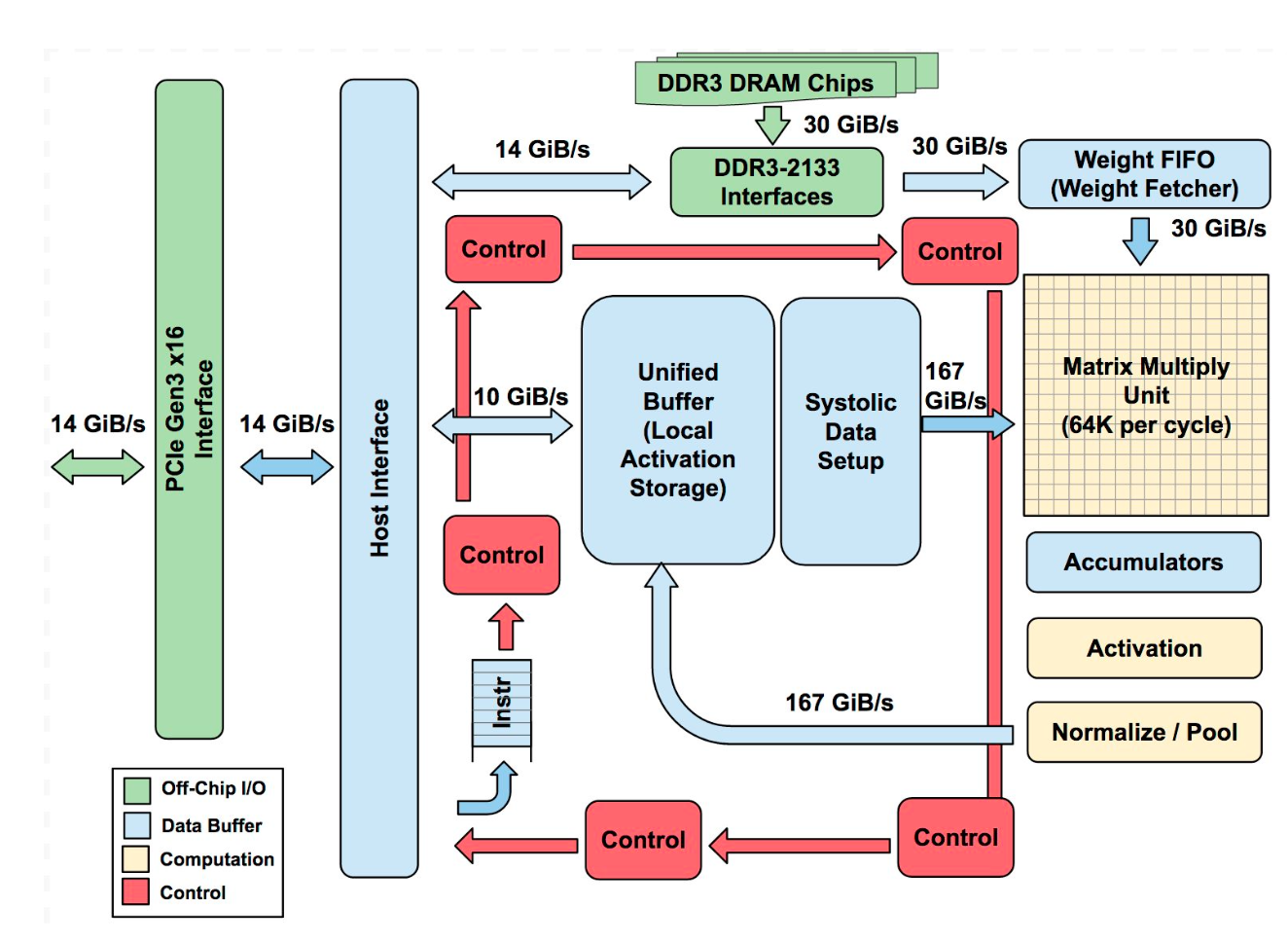
The main computation part is the yellow Matrix Multiply Unit (MXU) in the upper right hand corner. Its inputs are the blue Weight FIFO and the blue Unified Buffer (UB) and its output is the blue Accumulators (Acc). The yellow Activation Unit (AU) performs the nonlinear functions on the Acc, which go to the UB.
The main componnets are:
- Matrix Multiplier Unit (MXU): 65,536 8-bit multiply-and-add units for matrix operations
- Unified Buffer (UB): 24MB of SRAM that work as registers
- Activation Unit (AU): Hardwired activation functions
Key components
Matrix Multiplier Unit (MXU)
At least in TPU v1, each MXU performs 16K multiply-accumulate operations in each cycle using BF16 precision (16 bits with value cover the range of FP32 but in lower precision) for the internal multiplication and FP32 for accumulation.
Floor plan of TPU die
Because general-purpose processors such as CPUs and GPUs must provide good performance across a wide range of applications, they have evolved myriad sophisticated, performance-oriented mechanisms. As a side effect, the behavior of those processors can be difficult to predict, which makes it hard to guarantee a certain latency limit on neural network inference.
In contrast, TPU design is strictly minimal. You can see its simplicity in the floor plan of the TPU die.
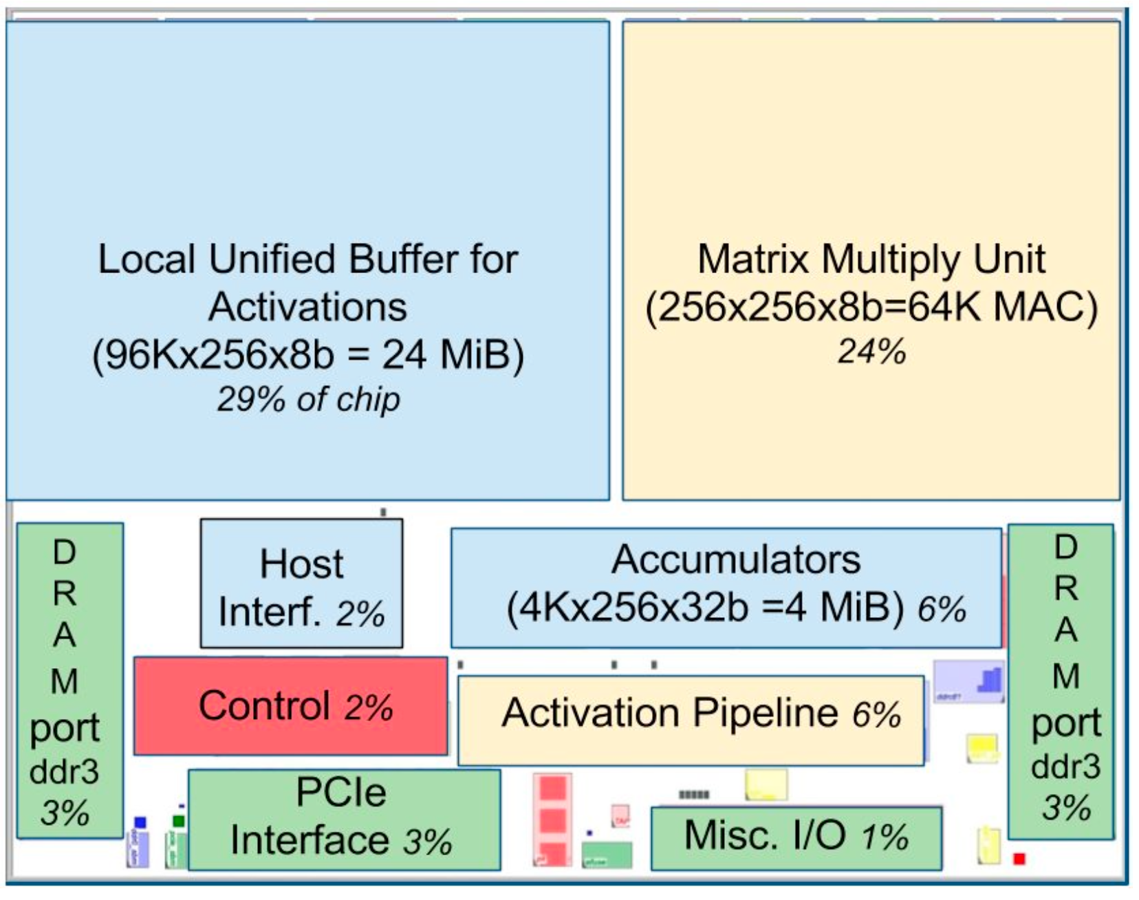
(yellow = compute, blue = data, green = I/O, red = control)
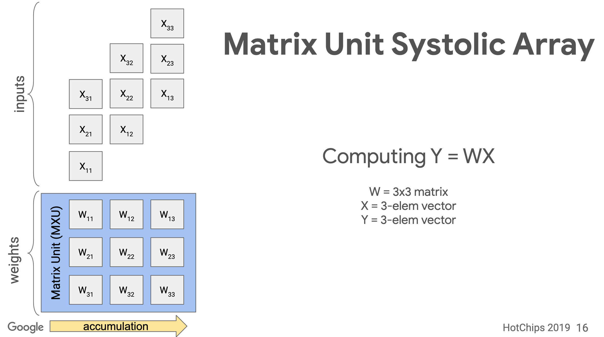
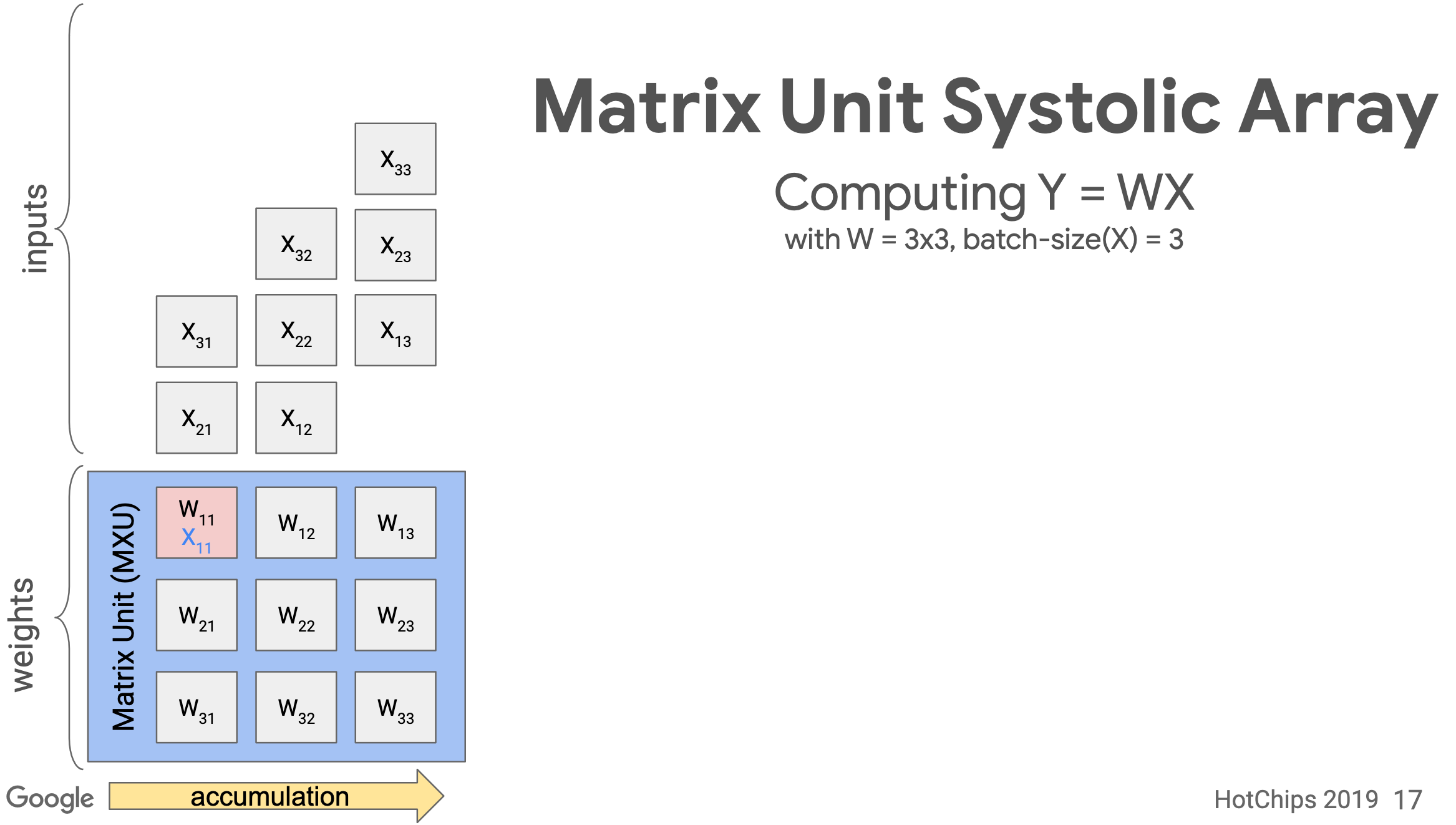
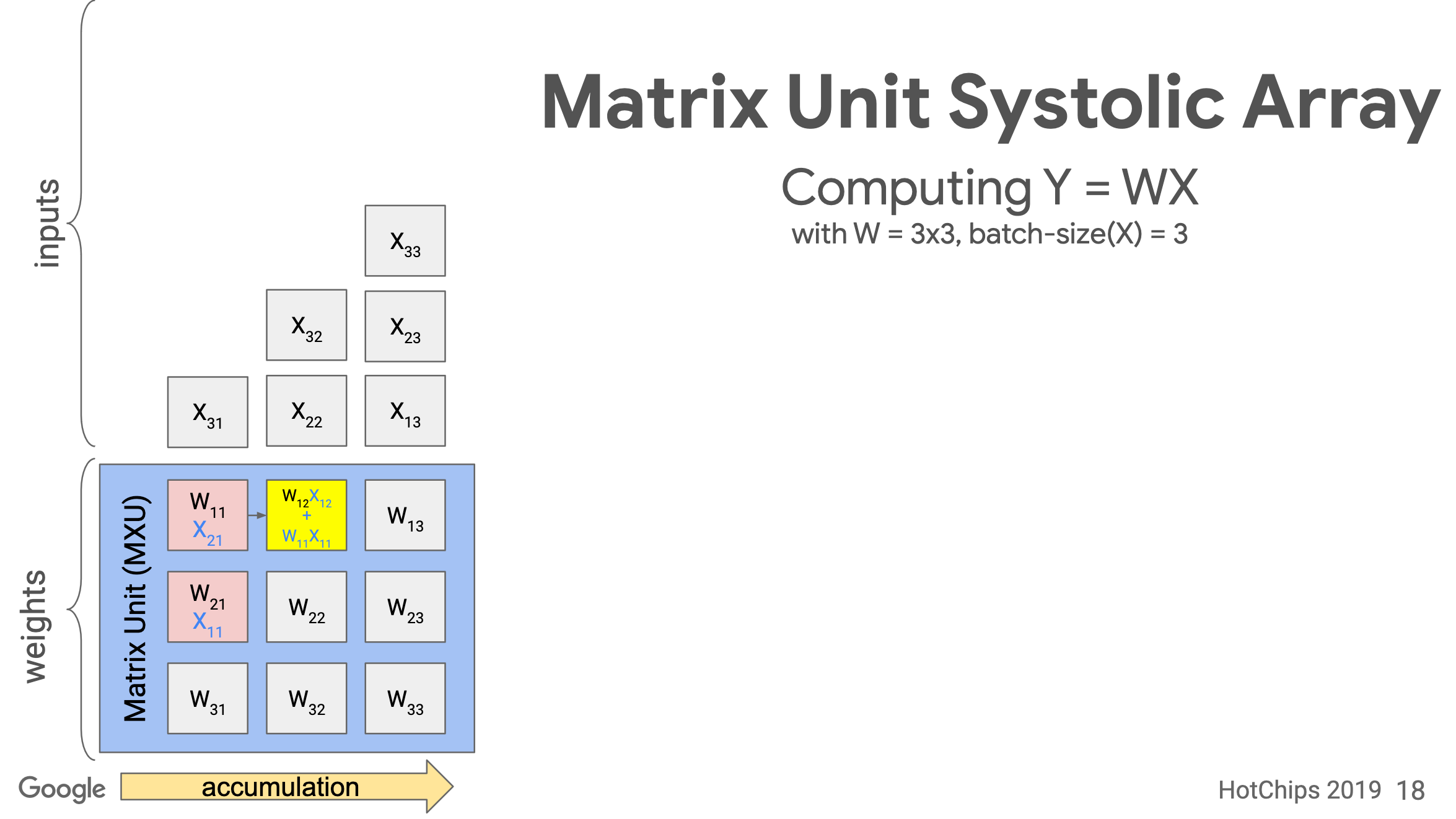
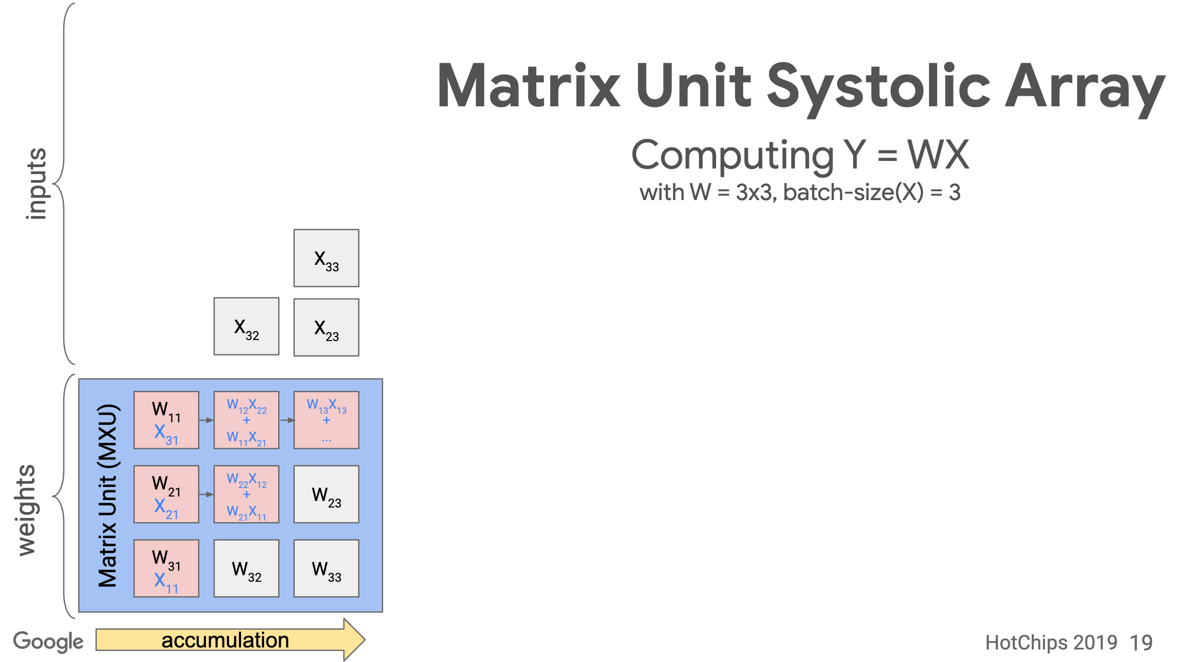
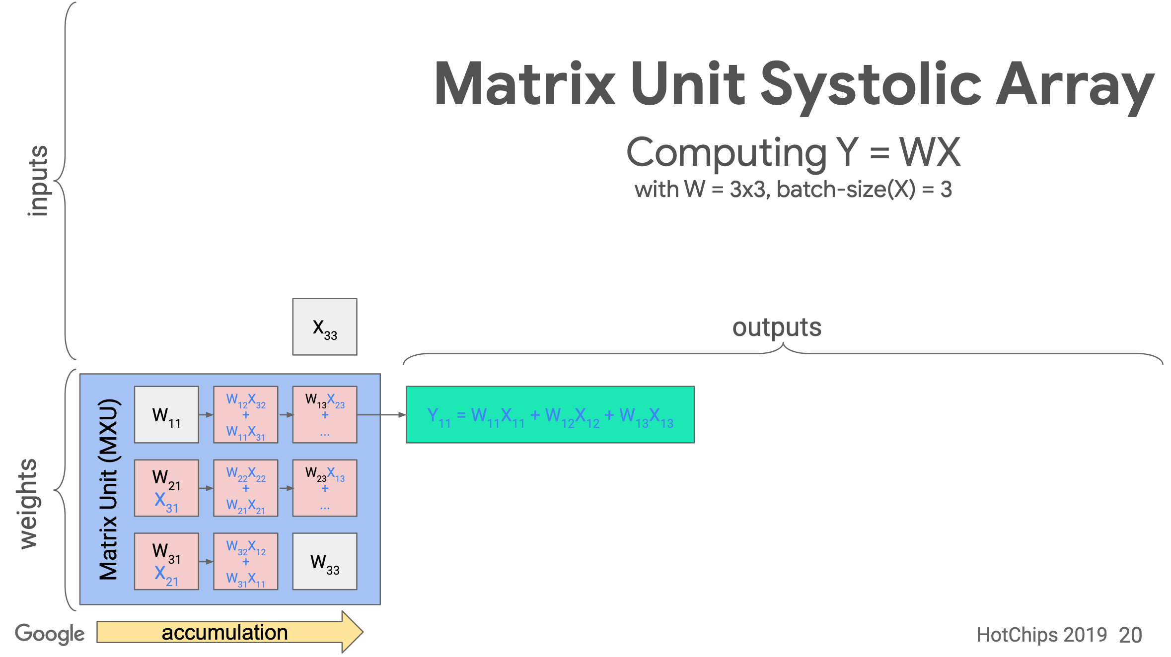
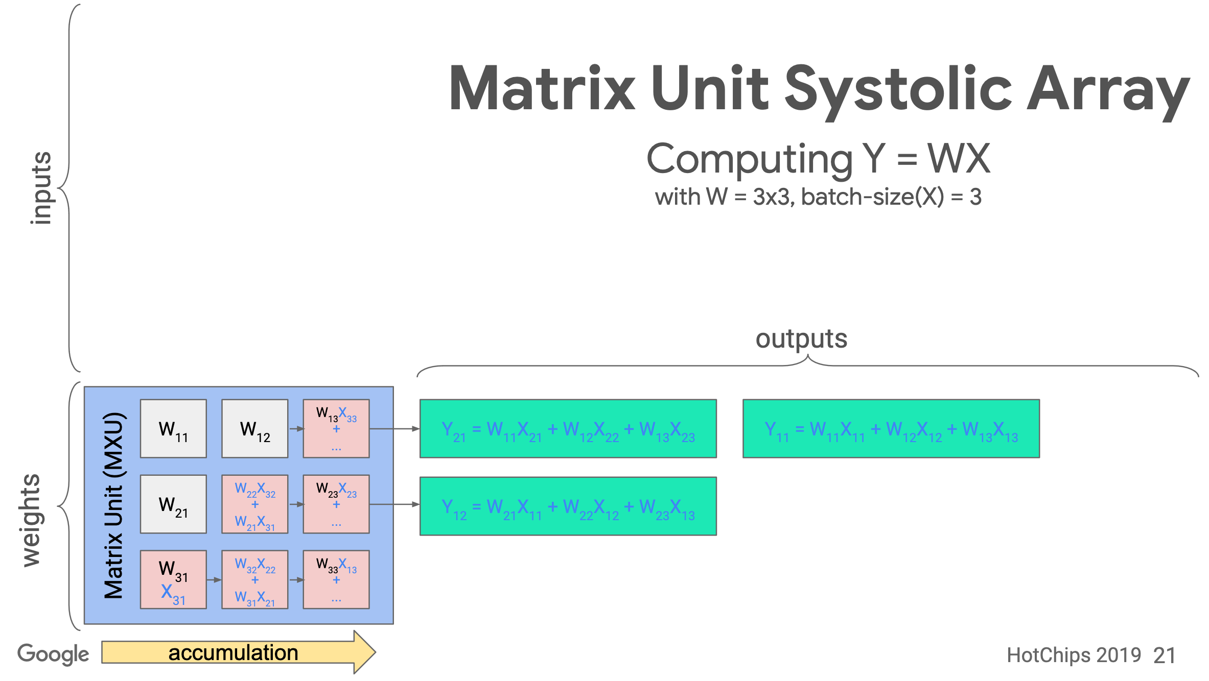
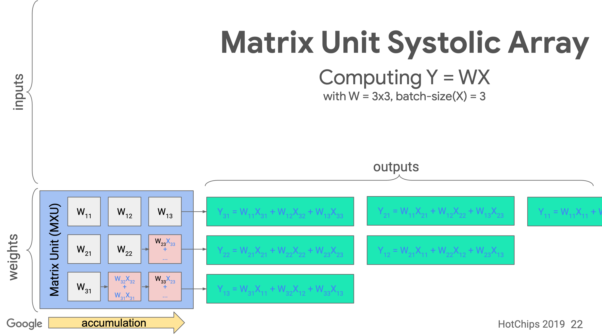
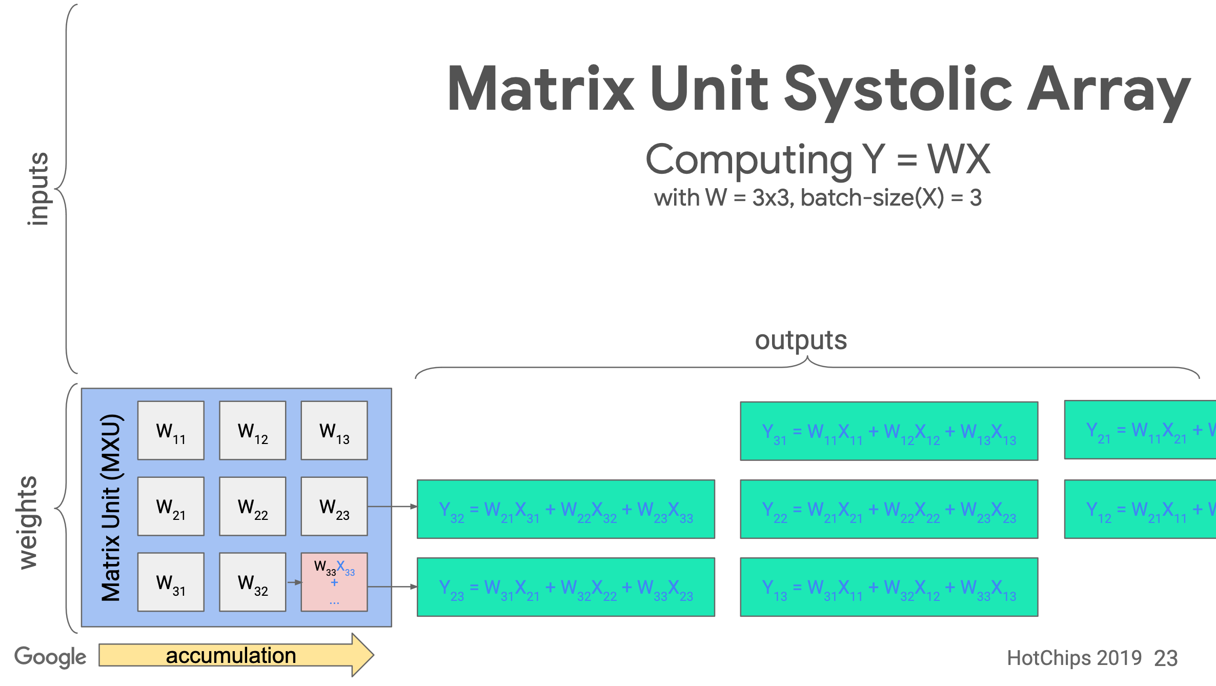
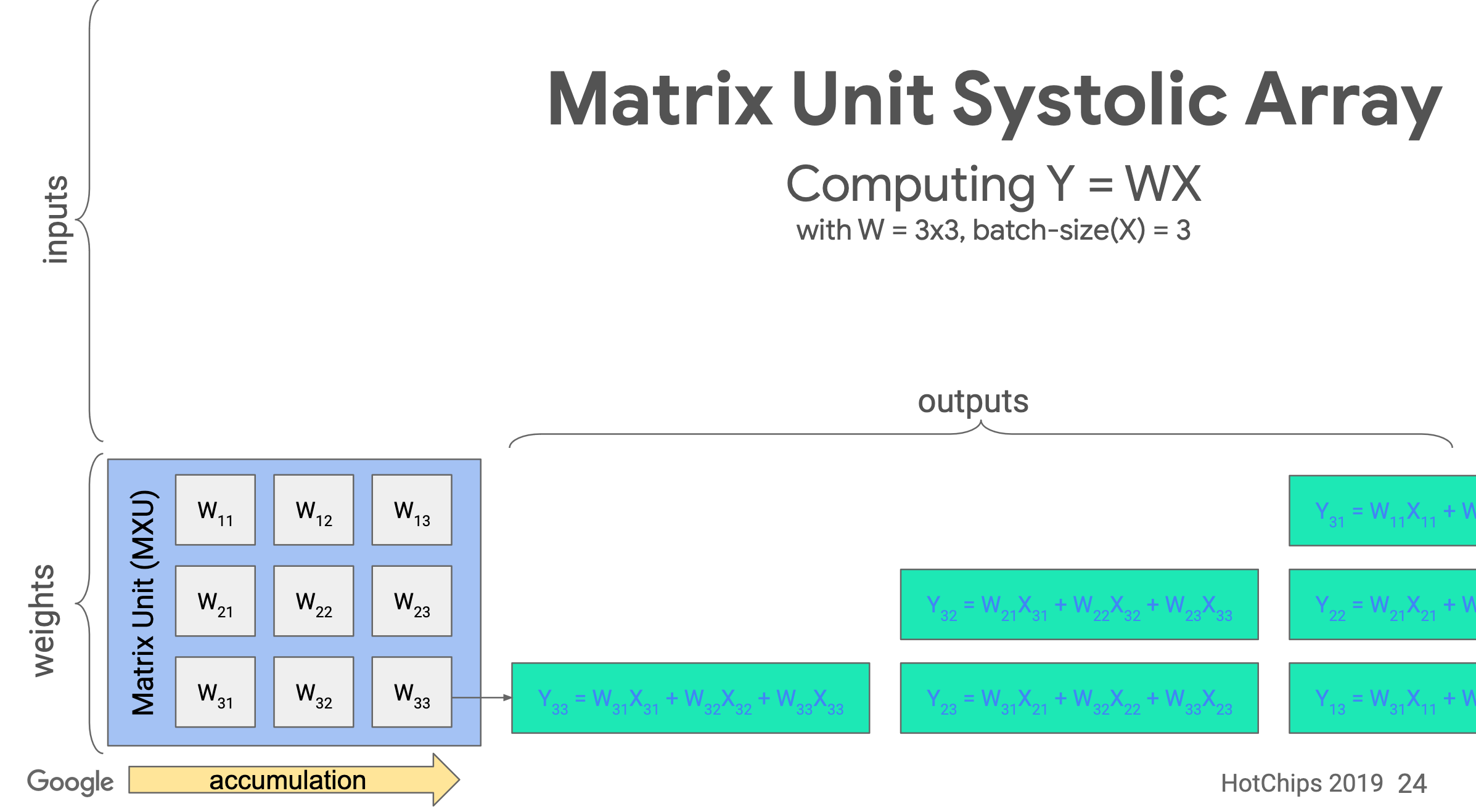
Systolic array
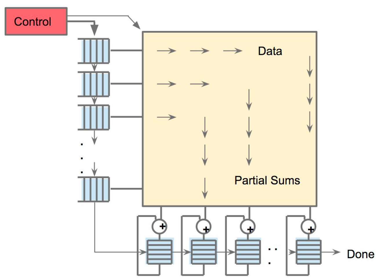
TPU implements the Matrix Unit (MXU) with the systolic array in a pipeline fashion.
In TPU v1, the MXU is a 128 x 128 systolic array. Below is the processing logic of a systolic array. Images are from ->source.
Load the values of a matrix
t=1
t=2
t=3
t=4
t=5
t=6
t=7
t=8
Technogies
Quantization in neural networks
"If it’s raining outside, you probably don’t need to know exactly how many droplets of water are falling per second — you just wonder whether it’s raining lightly or heavily. Similarly, neural network predictions often don't require the precision of floating point calculations." (Source)
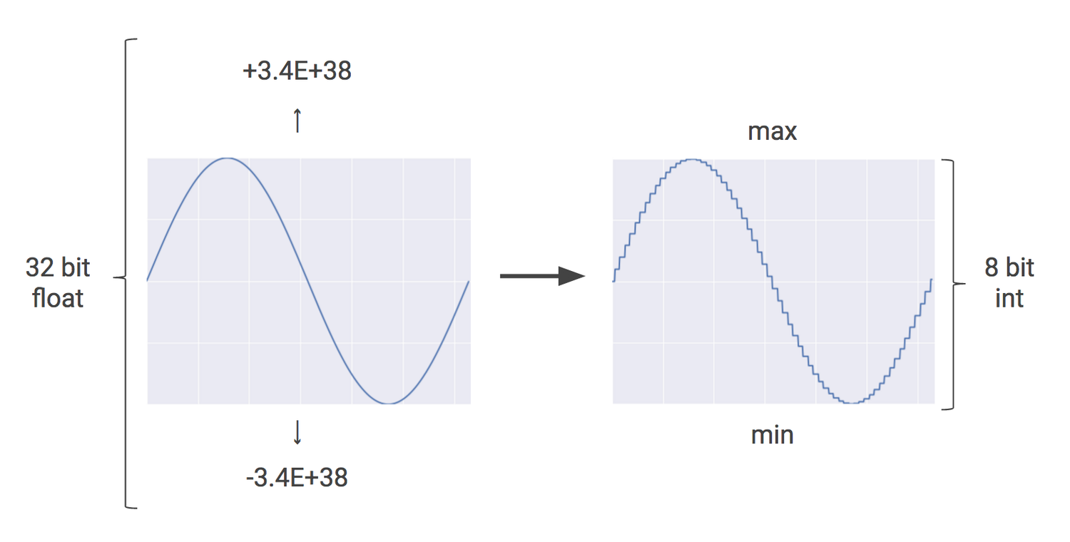
Quantization: Before inference phase, Google will apply an extra step called quantization transforms floating-point numbers into narrow integers—often just 8-bit integers—which are usually good enough for inference.
The idea is that 8-bit integers are usually good enough for inference.
The TPU instruction set
Since TPU is highly specilized, it has a lot of instructions dedicated for neural networks. As a result, it uses a Complex Instruction Set Computer (CISC) design, instead of the popular Reduced Instruction Set Computer (RISC) design.
TPU v1 defined a dozen high-level instructions. Five of these operations are highlighted below.
| TPU Instruction | Function |
|---|---|
| Read_Host_Memory | Read data from memory |
| Read_Weights | Read weights from memory |
| MatrixMultiply/Convolve | Multiply or convolve with the data and weights,accumulate the results |
| Activate | Apply activation functions |
| Write_Host_Memory | Write result to memory |
Pitfalls
Ideas that didn't fly for general-purpose computing may be ideal for domain-specific architectures.
For the TPU, three important architectural features date back to the early 1980s: systolic arrays, decoupled-access/execute, and CISC instructions. The first reduced the area and power of the large matrix multiply unit, the second fetches weights concurrently during operation of the matrix multiply unit, and the third better utilizes the limited bandwidth of the PCIe bus for delivering instructions. Historyaware architects could have a competitive edge.